Company History

Founded as a small family business, GS has evolved into the largest PCB manufacturer in Switzerland and a global leader in miniaturized printed circuit boards. With a dedicated team of approximately 200 employees and annual sales exceeding $50 million, we have positioned ourselves at the forefront of technological innovation. Our success is driven by continuous investments in state-of-the-art equipment and cutting-edge technology, ensuring we remain at the vanguard of technology.

Abstract modern white spiral clock.
1981

Establishment of GS Präzisions AG

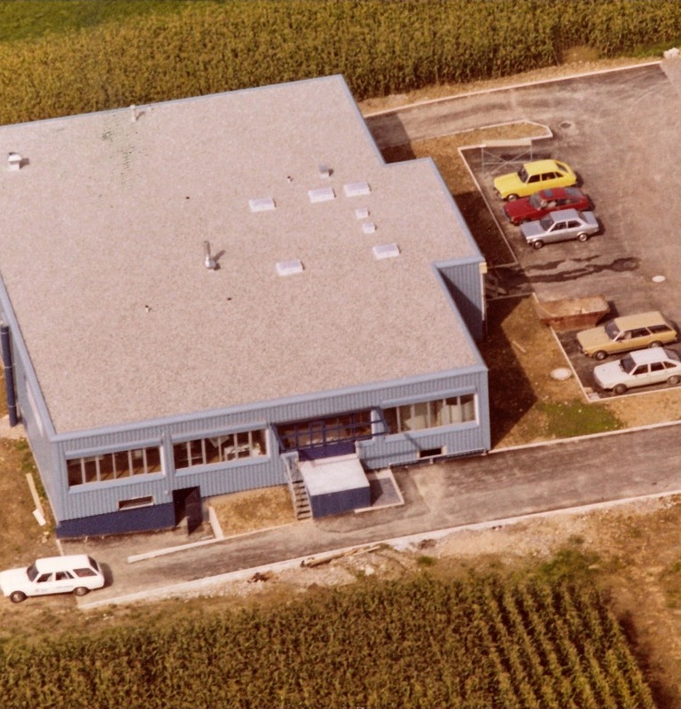
In the heart of Switzerland, Mr. and Mrs. Nerpas founded GS Präzisions AG in Kuessnacht am Rigi. The company started operation in a 600 m2 production facility with a dedicated team of five employees.

Aerial view of GS building captured in 1981.
1986

First Expansion of Production Facility

The production area was expanded to 1200 m2, and the workforce grew to 33 employees.

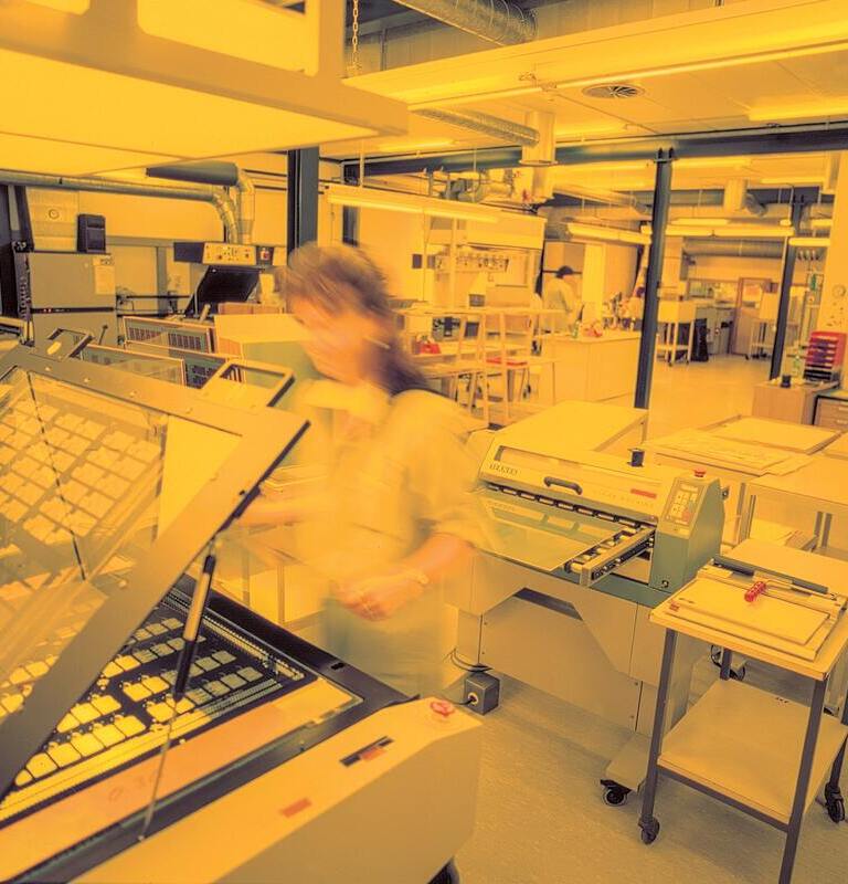
Exposer Unit in the photo department.
1989

Second Expansion with New Building Addition

A new building was added, increasing the total area to 2400 m2 and expanding the workforce to 45 employees.

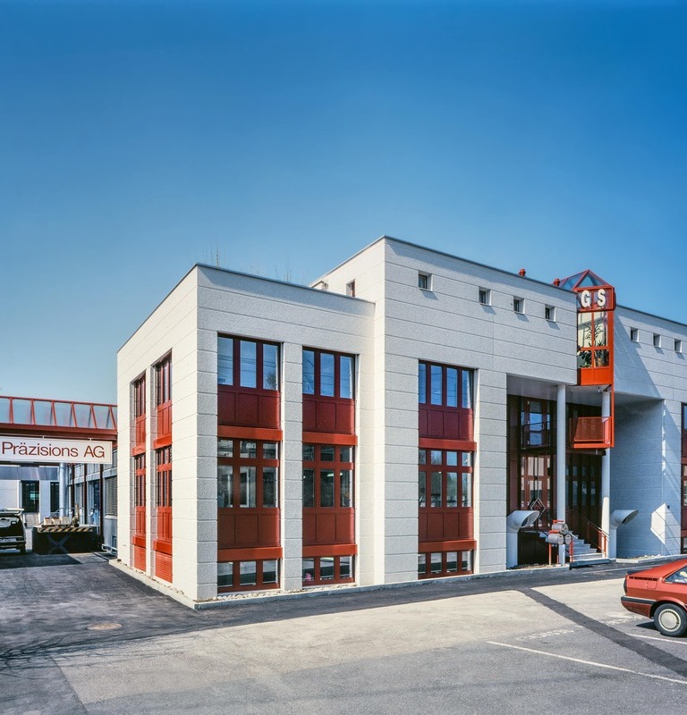
View of GS building captured in 1989.
1992

Integration of PCB Division of Landis + Gyr

GS Präzisions AG took over the PCB division of Zug-based Landis + Gyr, including 35 employees, equipment, and purchase orders.

Hands of business people celebrating successful company merger in office over plans lying on table.
1993

Third Expansion Completed

The production area increased to 4800 m2, and the work force expanded to 83 employees.

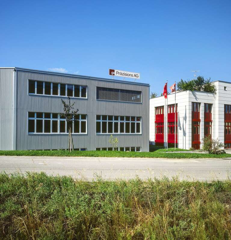
View of GS building captured in 1993.
1994

ISO 9001 Certification

GS Präzisions AG introduced a systematic and effective quality management system, achieving ISO 9001 certification.

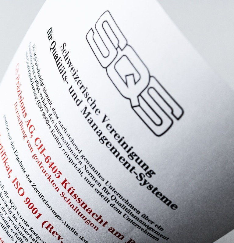
Photo of first ISO 9001 certificate obtained in 1994.
1995

Introduction of Flex and Rigid-Flex PCBs

The company began manufacturing flexible and rigid-flexible printed circuit boards, opening new markets and customer opportunities.

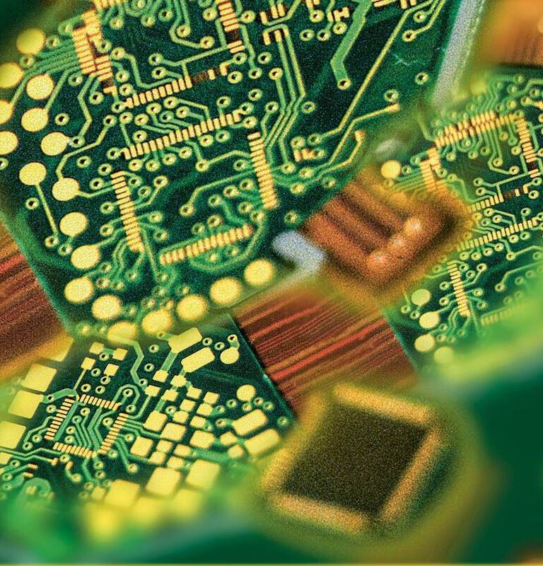
Several rigid-flex PCBs
2000

First Laser Machine

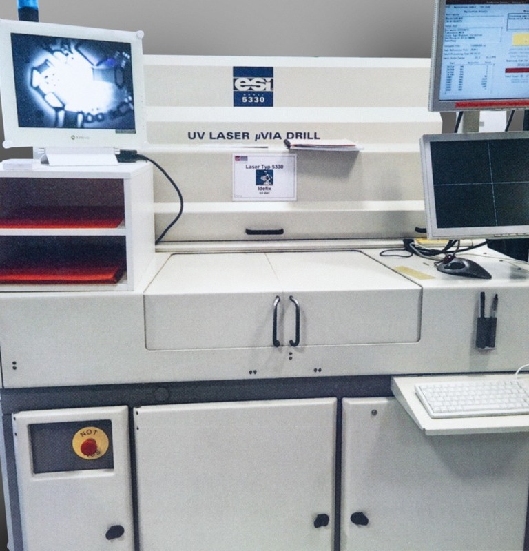
The introduction of laser drilling and cutting significantly increased precision, enabling the drilling of holes that were not possible with conventional mechanical drilling.

UV-Laser
2006

Acquisition by AEM Technologies Holding AG

After 25 years, the founder, Mr. and Mrs. Nerpas, sold the company to AEM Technologies Holding AG, an European group specializing in electronic components and products.

Low angle view of a large group of happy entrepreneurs joining their hands in unity and looking at the camera.
2007

LDI and Clean Room Milestone

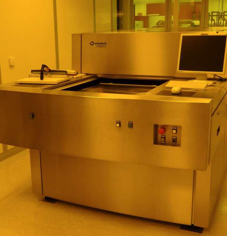
The use of Laser Direct Imaging (LDI) machines in a clean room marked a significant achievement in miniaturization and precision for producing dense patterns of solder mask and copper traces.

LDI in a cleanroom
2008

Name Change to GS Swiss PCB AG

To enhance brand recognition and international appeal, the company was renamed GS Swiss PCB AG.

Updated logo featuring the new company name GS Swiss PCB.
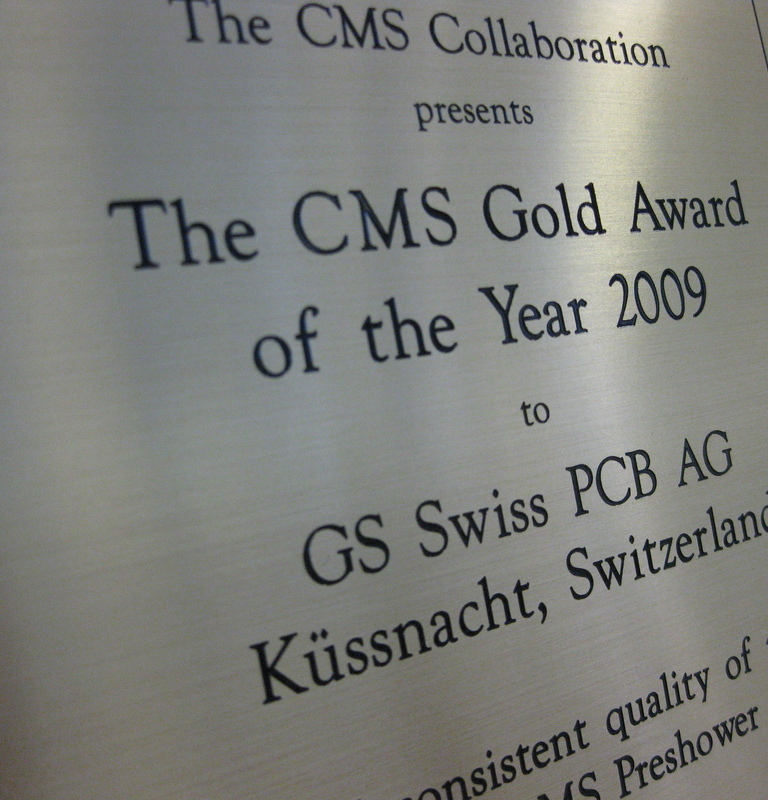
2009

CMS Gold Award

Award for the excellent and consistent quality of the PCBs supplied to CERN

CMS Gold award presented to GS Swiss PCB by CERN in 2009.
2010

Integration into exceet Group and Revenue Milestone

GS Swiss PCB AG exceeded revenues of CHF 30 million. The parent company, AEM Technologies Holding AG, was integrated into the Exceet Group and listed on the Frankfurt Stock Exchange.

Group of businessmen in the office, two of them shake hands for successful business, colleagues applaud.
2015

Establishment of Sales Office in Boston Area

To better serve US customers, a sales office was established on the East Coast, in the Boston area.

Boston down town.
2019

Forth Expansion and Addition of Two More Clean Rooms

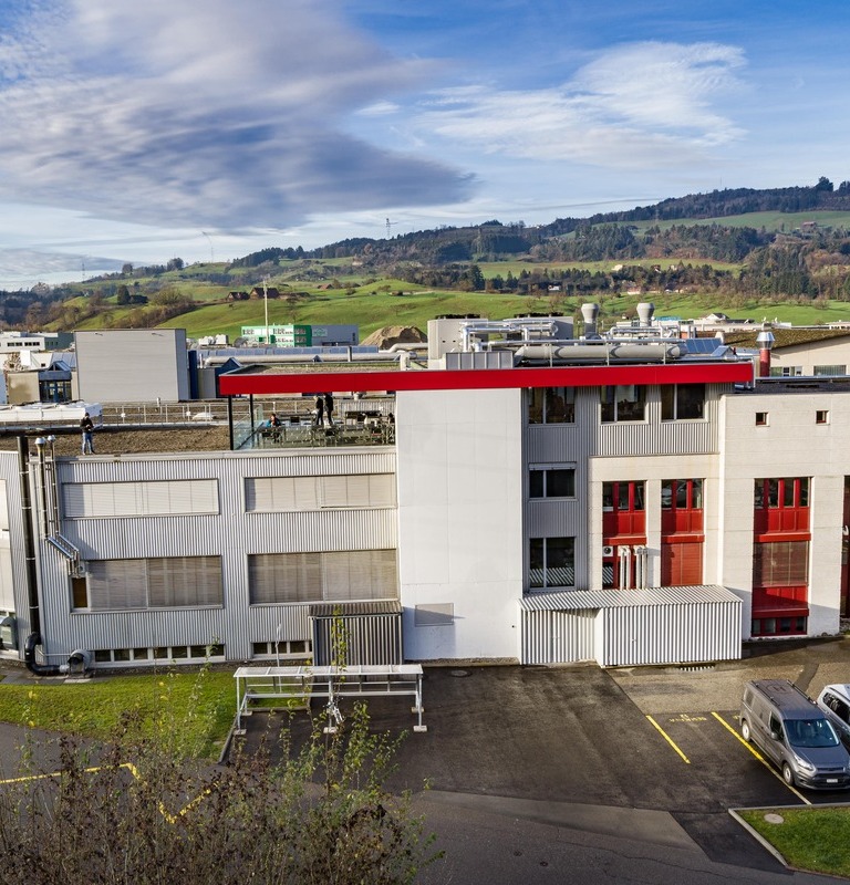
The production increased to 5600 m2 with two additional clean rooms, bringing the total to four. The number of employees rose to 164.

View of GS building after fourth expansion in 2019.
2020

Introduction of Semi-Additive Process (SAP)

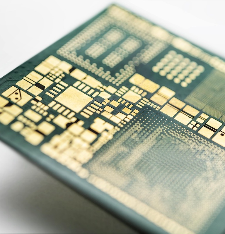
The SAP process revolutionized miniaturization, enabling the production of very small tracks, previously not possible to manufacture with conventional subtractive processes.

Substrate-like PCB (SLP) manufactured with SAP-technology.
2020

New GS Logo

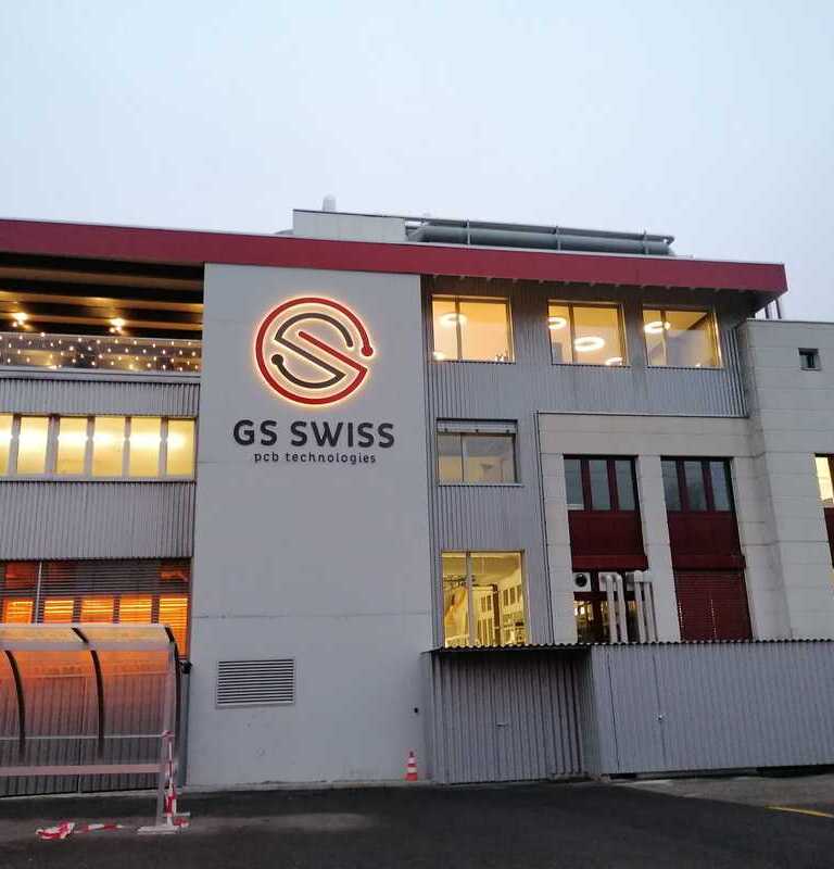
Introduction of a refreshed company design, featuring a modernized logo for a more contemporary look.

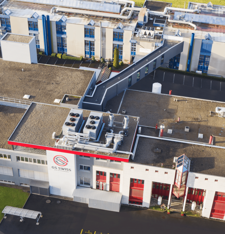
View of GS building with new circular GS Logo captured in 2020.
2021

Acquisition by STG Swiss Technology Group and Revenue Milestone

Afinum, a private equity company, acquired GS Swiss PCB through its holding company, STG Swiss Technology Group, with revenues exceeding CHF 40 million.

Unfocused shot of two businessmen shaking hands in an office.
2023

Hofstetter PCB AG Joins STG Swiss Technology Group

Hofstetter PCB AG, the largest plating house in Europe and a key partner and supplier since the beginning, became a sister company, strengthening cooperation and improving the supply security of plating services.

Aerial view of GS and Hofstetter PCB building captured in 2023.
1981
1986
1989
1992
1993
1994
1995
2000
2006
2007
2008
2009
2010
2015
2019
2020
2020
2021
2023

Scroll

+-cookies-eu-details

Cookie Settings

We use cookies to offer you an optimal user experience. Some cookies are necessary for the operation of the site, others are used for statistical purposes, comfort settings, or to display personalized content. You can decide for yourself which cookies you want to allow. Please note that your settings may mean that not all functions of the site are available. Further information can be found in our privacy policy and cookie policy.

Show details