mSAP & SAP

Modified Semi-Additive Process (mSAP) and Semi-Additive Process (SAP)

The traditional method of manufacturing printed circuit boards (PCBs) relies on subtractive technology. While this method remains prevalent, the increasing demand for miniaturization has highlighted its limitations, particularly regarding the minimum spacing between copper traces. As these distances shrink, production yields tend to decrease due to physical constraints.

Innovations in modified Semi-Additive Process (mSAP) and Semi-Additive Process (SAP) technologies have overcome these obstacles, enabling the production of highly miniaturized PCBs with high yields. The minimum conductor spacing achievable also depends on the height of the copper used.

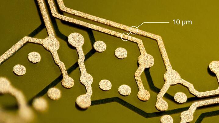
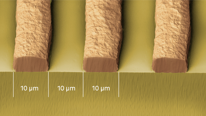
The subtractive method is limited to lines and spaces of 30 micrometers. In contrast, mSAP technology excels in line and space width ranging from 60 to 20 micrometers. SAP technology goes even further, allowing for lines and spaces as small as 10 micrometers and below.

Microsection of SAP flex PCB with 10 micrometers lines and spaces
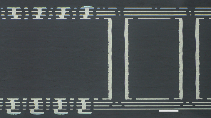
Microsection of IC-Substrate with 14 layers.

Applications of mSAP and SAP

mSAP and SAP technology are crucial for applications requiring extreme miniaturization, such as IC substrates and smartphones. These technologies are also essential for manufacturing products that need high signal density for superior resolution and precise imaging, like advanced ultrasound and MRI devices. In 5G infrastructure components, the precise shapes of conductors ensure the undistorted high-frequency signals necessary for advanced telecommunications.

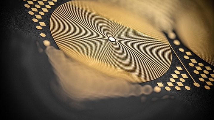
SAP-PCB with coil with 10 micrometers lines and spaces
Detail of rigid SAP-PCB with 10 micrometers lines and spaces. Name: Detail-rigid-PCB-SAP
To meet the evolving needs of its customers, GS began developing SAP technology and investing in state-of-the-art equipment and cleanrooms in 2019.

From the outset, GS has been committed to mastering SAP technology for both flexible and rigid PCBs. In spring 2024, GS commenced serial production of flexible PCBs utilizing SAP technology, achieving lines and spaces as fine as 10 micrometers.

Advantages of mSAP and SAP Technology

Fine Line Capability

mSAP and, to an even greater extent, SAP technology enable the manufacturing of dense patterns that are unachievable with conventional subtractive methods. This advancement allows for the creation of highly miniaturized products that were previously not possible.

Improved Performance

SAP technology provides exceptional control over trace geometry and spacing, resulting in nearly rectangular cross-sections and smooth surfaces. This precision ensures consistent electrical characteristics across the board and minimizes parasitic effects, which are crucial for optimal performance and signal integrity at high frequencies.

Versatility in Design

mSAP and SAP technologies provide greater flexibility in circuit design, allowing for innovative and custom solutions tailored to specific applications. This can be a significant competitive advantage in developing new products.

Environmental Benefits

These technologies often require fewer materials and generate less waste compared to traditional subtractive processes, contributing to more sustainable manufacturing practices.

Three Distinct Manufacturing Methods: 
Subtractive, mSAP, SAP

1.

Subtractive Technology:

This traditional method begins with a fully copper-clad laminate. A structured photoresist covers the desired copper structure, protecting the underlying copper during the etching process. After stripping the photoresist, only the intended copper traces remain.

2.

Modified Semi-Additive Process (mSAP):

mSAP starts with a laminate that has a very thin copper layer, which is covered with a photoresist to define the circuit pattern. Additional copper is plated onto the exposed areas to build up the desired traces. After stripping the photoresist, the thin copper layer between the tracks is etched away, leaving the desired copper structure.

3.

Semi-Additive Process (SAP):

SAP uses a non-conductive substrate with an extremely thin copper layer (less than 1 μm) plated onto it. Copper is then built up only in the open areas defined by a precise photoresist pattern to form the desired structure. After stripping the photoresist, the very thin copper layer remaining between the tracks is etched away using flash etching, leaving the desired copper pattern.

Process Steps: Subtractive – mSAP - SAP

Cross Section Characteristics

Subtractive:

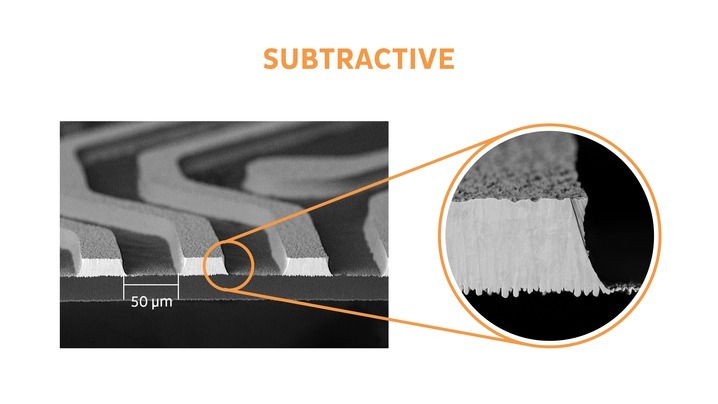
The traces have a trapezoidal cross-section because the etching process removes copper from the top and sides of the traces. This leads to wider traces at the base than at the top.

mSAP:

The traces have a more rectangular cross sections compared to the subtractive process.

SAP:

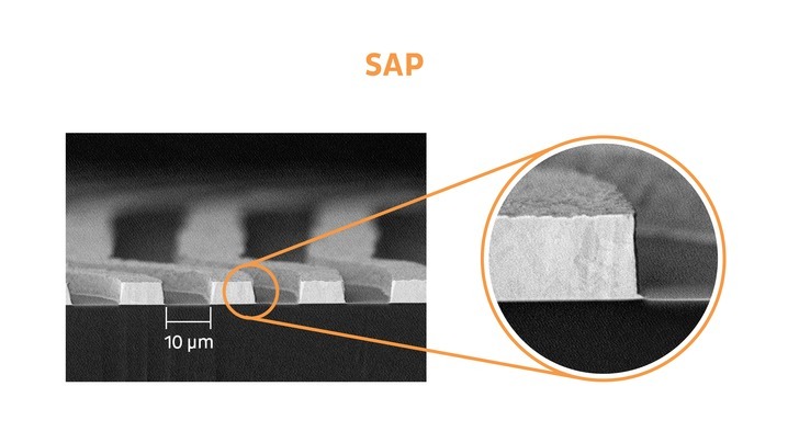
The traces have nearly perfect rectangular cross-sections with sharp and defined edges. SAP offers the best control over dimensions and trace geometry among the three manufacturing methods.

Microsection of traces manufactured with subtractive Technology.
Microsection showing the flank of a trace manufactured with SAP Technology.
Unlock the Power of SAP-Technology

Contact us today to explore the full potential of mSAP and SAP technology.

+-cookies-eu-details

Cookie Settings

We use cookies to offer you an optimal user experience. Some cookies are necessary for the operation of the site, others are used for statistical purposes, comfort settings, or to display personalized content. You can decide for yourself which cookies you want to allow. Please note that your settings may mean that not all functions of the site are available. Further information can be found in our privacy policy and cookie policy.
Show details