We use cookies in order to optimize your user experience. Several cookies are necessary to
operate the site, while others are used for statistical purposes, to provide user-friendly
settings, or to display personalized content. You can decide for yourself which cookies you
wish to allow. Please note that some of the site’s functions may be unavailable as a result
of your settings. You can find further information in our data privacy statement.
Show details
Flex PCB
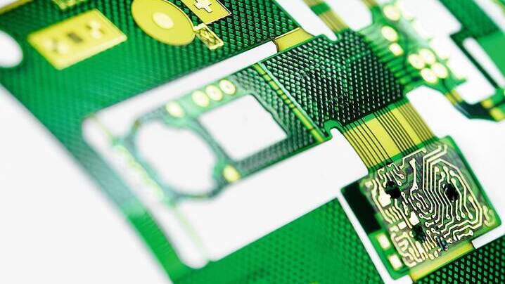
GS Swiss PCB AG is a specialist for miniaturization and offers a broad range of highly integrated (HDI) printed circuit boards with blind and buried vias. Our capabilities include copper filled micro vias as well as surface finishes that can be bonded and assembled with high yields. Complex contours and depth milling can be realized with narrow tolerances. Our HDI-substrates can be found mainly in applications where high quality and reliability are of paramount importance.
High degree of miniaturization thanks to system in package (SiP) on flexible substrate
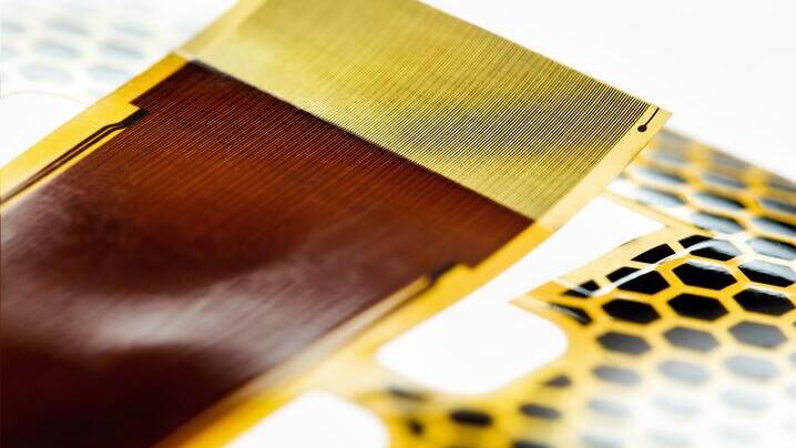
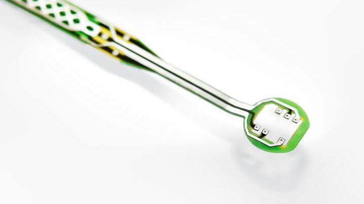
This 65 µm thin flex PCB (electromechanical thickness) is folded three times and sealed after being assembled with bare dies (COF) and small SMD-components. This allows the realization of a complex electronic design with digital signal processing requiring minimum space and exhibiting maximum form factor. Various electronic functions are combined in this BGA type housing to form a custom specific electronic component (SiP).
3-layer flexible substrate for hearing instrument
The flexibility of the substrate is varied by removing the outer metal layers on this substrate which is about 150 µm thick. Where all three metal layers are present, the substrate is more rigid and components are easily assembled, while the flex bending zones enable complex 3D shapes during final assembly.
Flex PCB as substitute for cables
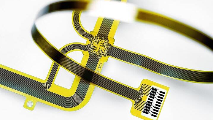
This two layer flex circuit joins three arms with a rigidized center piece without the use of any connectors and therefore increases the reliability substantially. At the same time the assembly cost is lowered and the number of components reduced. The dimensions of this PCB are 532 x 77 mm.